Functional oxides are a class of highly correlated materials displaying many different phenomena such as ferromagnetism, antiferromagnetism, ferroelectricity, piezoelectricity and superconductivity, with a strong interplay between them. For this reason they have attracted a lot of attention, in view of the possibility to introduce novel functionalities in electronic devices, beyond those provided by conventional semiconductor materials. In this framework the NaBiS group is currently working on the study of phenomena and architectures for the implementation of novel non-volatile memory devices involving ferroelectric and ferromagnetic materials.
A relevant research topic deals with the investigation of artificial multiferroic systems, made of ferromagnetic and ferroelectric materials with some coupling between the ferroelectric polarization and the magnetization, allowing to control the magnetic properties via an electric field or the ferroelectric state via a magnetic field. Thanks to the so-called “magnetoelectric coupling” it is then possible to design novel magnetic memories where the writing of the information is performed by applying an electric field. This represents a viable route to solve the well known problem of the energy dissipation during the magnetic writing, even beyond the current spin transfer torque technology, still requiring current densities as high as 106 A/m2.
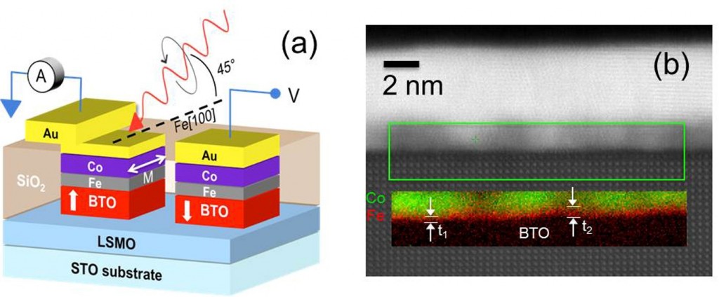
Our research focuses on the magnetoelectric coupling of thin magnetic films (few nanometers thick) of 3d-metals and alloys (such as Fe and CoFeB), with in-plane or out-of-plane magnetization, grown by molecular beam epitaxy and magnetron sputtering, on BaTiO3 (100) films, grown by pulsed laser deposition in a MBE/PLD cluster tool. This constitutes a prototypical interface between a ferromagnet and a well-known piezo-ferroelectric material. Our group has been the first capable of growing high quality epitaxial Fe films on BaTiO3 to be used for detailed investigations of the interfacial magnetoelectric coupling. By employing magneto-electric and magneto-optic characterization tools, also in collaboration with external institutions (Elettra – Trieste, and ICMAB – Spain), we explored the interplay between the ferroelectric polarization of BaTiO3 and the magnetic properties (magnetic moment, coercive field, magnetic order) of the ferromagnetic side of the Fe/ BaTiO3 interface. In particular we demonstrated the room temperature, reversible electric switching of the interfacial Fe magnetization. This result recently lead to the electrical control of the TMR in magnetic tunnel junctions grown onto BaTiO3 films. In case of CoFeB films on BaTiO3, we have showed the possibility of reversibly and electrically switching the magnetization of the CoFeB films displaying perpendicular magnetic anisotropy, in bias magnetic fields as low as 10 Oe.
A second topic deals with the investigation of ferroelectric tunnelling junctions (FTJs), i.e. tunnelling junctions where the tunnelling barrier is ferroelectric, so as to display a huge variation of the resistance for opposite states of the ferroelectric polarization. This phenomenon, called Tunneling Electroresistance (TER), has been proposed to realize non-volatile memories and also memristive devices for neuromorphic computing.
In collaboration with the group of Prof. Fontcuberta in ICMAB, we have recently demonstrated the capability of fabricating micron sized FTJs with record values of the TER (up to 106) and clarified the role of an interfacial n-doped layer in the BaTiO3 barrier to understand the voltage modulation of the device resistance. More recently we have also contributed to the demonstration of the optical reading of the ferrolectric state in n-doped BaTiO3 films embedded in microcapacitors.

References
[bibtex file=http://nabis.fisi.polimi.it/data/bib/functional_oxides7.bib format=ieee key_format=numeric process_titles=0]
Involved People
- Lorenzo Baldrati
- Marco Asa
- Christian Rinaldi
- Matteo Cantoni
- Riccardo Bertacco (corresponding person)
Related projects
This research has been supported by the Cariplo Foundation via the project EcoMag and by MIUR via the project FIRB “Ossidi nano strutturati: multifunzionalità e applicazioni” (RBAP115AYN).